 Warning
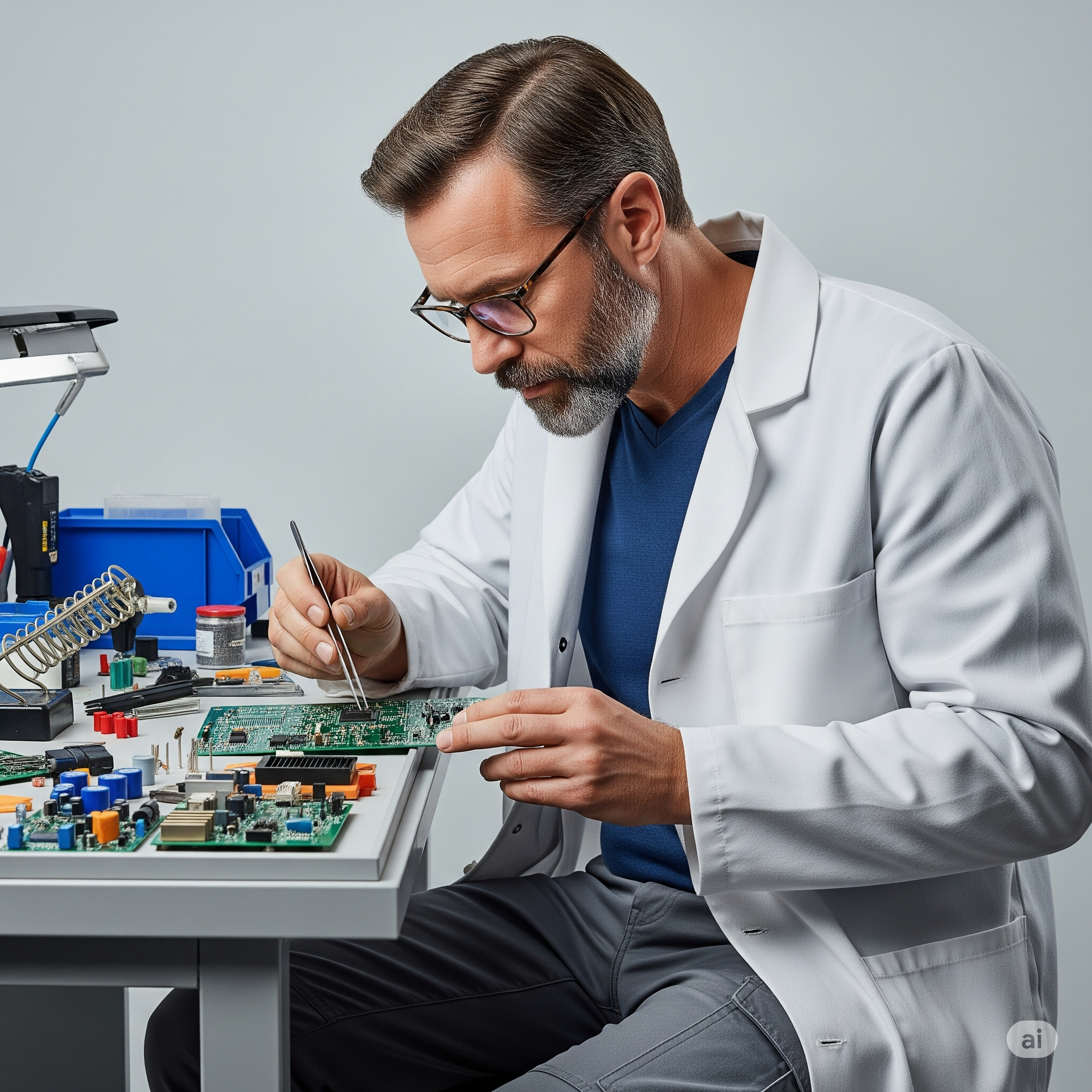
Blog
Developing a Reliable and Functional Printed Circuit Board (PCB): A Step-by-Step Guide for PCB Developers
Developing a reliable and functional printed circuit board (PCB) involves several methodical and interdependent steps. Whether you are a startup building your very first prototype or a seasoned PCB developer refining a complex design, understanding and executing each phase with precision is critical. A well-designed PCB is the backbone of any electronic product, influencing performance, durability, cost, and scalability.
1. Circuit Design and Schematic Capture
PCB development starts with circuit design. In this stage, the PCB developer defines the system’s logic and behavior by carefully selecting components and organizing them into a schematic and using professional CAD tools like Altium Designer, Eagle, or KiCAD, the schematic maps every system’s resistor, capacitor, microcontroller, and connection.
Accuracy here is non-negotiable. A small error (like a misplaced ground connection or incorrect resistor value) can cascade into significant performance issues later. Early collaboration with electrical engineers and a clear understanding of the final application help ensure a robust design foundation.
2. PCB Layout and Routing
With the schematic complete, the focus shifts to PCB layout and routing, where the design becomes a physical blueprint. The PCB Developer places each component on the board, considering not just functionality but also thermal performance, manufacturability, and electromagnetic compatibility (EMC).
Routing the copper traces is a delicate art. Proper trace width, spacing, and layer stacking are essential for signal integrity, especially in high-frequency applications. Ground planes and power distribution must be optimized to minimize noise and voltage drops. Good routing can also simplify debugging and enhance long-term reliability.
3. Design Rule Check (DRC) and Verification
Before moving forward, the layout undergoes a Design Rule Check (DRC). This automated process ensures that all elements meet the manufacturer’s specifications (like minimum trace width, via sizes, and component spacing).
Beyond DRC, advanced simulations such as signal integrity analysis, power integrity checks, and thermal modeling can be performed. These allow PCB developers to proactively catch and resolve potential issues, reducing costly iterations later.
4. Fabrication
Once the design is verified, it is time to send the files to a fabrication house. This stage involves converting digital layouts into physical boards using materials like FR-4, polyimide, or metal-core substrates, depending on the application’s needs.
Key considerations include the number of layers, copper weight, surface finish (HASL, ENIG, etc.), and penalization for mass production. Choosing a reputable fabrication partner ensures the boards are exact, avoiding defects like delamination, misalignment, or impedance mismatches.
5. Assembly and Testing
After fabrication, the bare boards move to the assembly phase. Here, components are soldered onto the board using surface mount technology (SMT) or through-hole soldering, depending on the component types.
Following assembly, rigorous functional testing is performed. PCB Developer, power up the board and run diagnostic routines to verify that each section behaves as expected. Debugging and rework are initiated to correct the faults if issues are found, such as short circuits, non-functional components, or signal noise.
6. Final Validation and Quality Assurance
Before the PCB can be integrated into its final product, it must undergo final validation. This includes environmental stress testing (such as thermal cycling or humidity exposure), mechanical stress tests (vibration or drop testing), and industry-specific compliance assessments.
Quality assurance is not optional but regulated in sectors like automotive, aerospace, and medical devices. Certifications like IPC standards or ISO compliance may be required, and extensive documentation must accompany the final product.
Each step in PCB development contributes to creating a board that is functional, reliable, efficient, and ready for production. For any PCB developer, mastering these stages is essential to delivering high-quality electronics that can meet the complex demands of today’s technology-driven world. From concept to finished board, precision and expertise make the difference.
Whether you’re an early-stage PCB developer or scaling a custom hardware solution — we’re here to help you build better, faster.
👉 Get a Quote Today
You can read more prototyping articles in the Warning Machines blog :